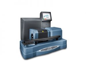
Field Emission Gun Scanning Electron Microscope with EDX Analyzer
A scanning electron microscope (SEM) produces images of a sample by scanning the surface with a focused beam of electrons. This provides information about the topography, composition and electrical conductivity of the sample.
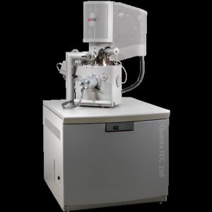
The FEG SEM facility is an ultra-high resolution field emission scanning electron microscope and is ideal for studying materials on the nanometer scale. The microscope is equipped with energy dispersive X-ray analysis (EDX).
Some important parameters are as under.
• Accelerating voltage 30 kV
• Magnification up to 1,000,000X
• EDX system with software library (liquid N2 free).
• Low vacuum mode pressure range 10 Pa to 300 Pa.
• A stage, which holds a sample size of at least 50mm x 50 mm
• Resolution range=0.8nm at 15kV.
X-Ray Diffractometer
X-ray Diffraction is a technique used for determining the atomic and molecular structure of a crystal, in which the crystalline atoms cause a beam of incident X-rays to diffract into many specific directions. By measuring the angles and intensities of these diffracted beams, a three-dimensional picture of the density of electrons within the crystal can be found. Key features include.
• Theta/theta (i.e. fixed sample) with 9 position sample changer
• Position sensitive detector (LynxEye) and standard detector (SC) with auto-absorber & graphite 2nd beam monochromator and sample rotation.
• Divergent beam, Bragg Brentano parafocusing geometry, reflection mode and most slit motorized (min step 0.0001° for detector & 0.0001° for tube (omega), best instrumental resolution ~0.08° in 2theta & ~0.04° in omega) for Thin film/powder samples.
• XRD analysis software facility with library.

Differential Scanning Calorimeter
The DSC 8000, double-furnace, power compensation DSC provides greater sensitivity and accuracy as well as faster and more reliable results. It can test specimens from sub ambient temperatures to above ambient temperatures.
Sample Experiments
• Isothermal kinetics studies of Polymers
• UV curing in polymers
• Determining the glass transition temperature of a polymer.

Dynamic Mechanical Analyzer
Dynamic Mechanical Analyser measures the mechanical properties of materials as a function of time, temperature, and frequency. DMA is commonly used to measure glass transition temperatures and secondary transitions, orientation caused by processing, cold crystallization, cure optimization, filler effects in composites.
Sample Experiments
• Measurement of a material’s stiffness modulus.
• Determination of the mechanical properties such as damping, creep, and stress relaxation.

Thermo-gravimetric analyzer with Evolved Gas Analyzer
A thermogravimetric analyzer continuously measures mass while the temperature of a sample is changed over time. This measurement provides information about physical phenomena, such as phase transitions, absorption and desorption; as well as chemical phenomena including thermal decomposition, and solid-gas reactions (e.g., oxidation or reduction).
It is a useful technique for the study of polymeric materials, including thermoplastics, thermosets, elastomers, composites, plastic films, fibers, coatings, paints, and fuels.

Sample Experiments
• To evaluate the thermal stability of a material
• To study the thermogravimetric kinetics for insight into the reaction mechanisms of thermal decomposition involved in the Pyrolysis and Combustion processes of different materials.
Simultaneous TGA/DSC
Simultaneous thermal analyzer measures the material temperature (or time) as a function of the heat flux and weight change under controlled atmosphere. The SDT Q600 provides a DSC-TGA measurement up to 1500 ° C.
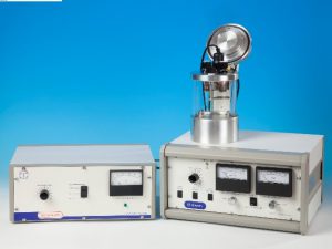

Au Sputter Coater with Carbon coating accessory
Sputter coating for SEM is the process of applying an ultra-thin coating of electrically-conducting metal – such as gold (Au), gold/palladium (Au/Pd), platinum (Pt), silver (Ag), chromium (Cr) or iridium (Ir) onto a non-conducting or poorly conducting specimen. Sputter coating prevents charging of the specimen, which would otherwise occur because of the accumulation of static electric fields. It also increases the amount of secondary electrons that can be detected from the surface of the specimen in the SEM and therefore increases the signal to noise ratio. The sputter coater is also used for quality thin film deposition.
The thermal evaporation of carbon is widely used for preparing specimens for electron microscopy. A carbon source in the form of a thread or rod is mounted in a vacuum system between two high-current electrical terminals. When the carbon source is heated to its evaporation temperature, a fine stream of carbon is deposited onto specimens.

Sample Experiments
• Au Sputtering on a non-conductive sample for SEM.
• Understanding the principles of thin film deposition on a substrate
• Carbon coating on a specimen for SEM